This thesis covers the design of a Folded Cascode CMOS Operational Amplifier Op-Amp in Raytheons 12-micron Silicon Carbide SiC process. The folded cascode op-amp uses silicon carbide transistors as it is intended to be used for high temperature applications ideally in the 25 C 300 C range.

Cmos Fully Differential Folded Cascode Opamp With A Large Step Applied Download Scientific Diagram
The simulation of the cascode and folded cascode circuits is done using TSPICE simulation tool and the LEVEL2 125 µm parameters are used.

. The design procedure is customized for using the OTA in a fully. In this paper we present a systematic and automated design flow for the most popular integrated circuit OTA architecture namely the folded cascode OTA. five folded cascode OTAs have been implemented spanning a bias range of 1 A-10 mA withmeasured unity-gain bandwidths within 20 of the designed value.
Design procedure of fully diferential folded cascode OTA. Folded-cascode Class-AB Operational Amplifier 4 2. Design procedure folded cascode the design procedure is simpleJust derive the kp and kn and lambda values from simulationThen do your hand calculations and then go for design.
The method has been applied in the design of a 3rd order receivers. Folded cascode OTA is a topology where differential input pair is connected to the output stage that implemented telescopic cascode topology. In 6 further enhancement in the DC gain and UGB of the RFC OTA is obtained using Improved Recycling structure and is termed as IRFC OTA.
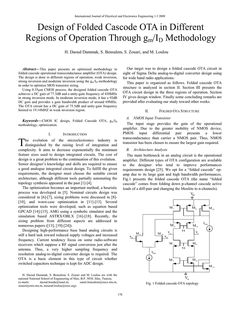
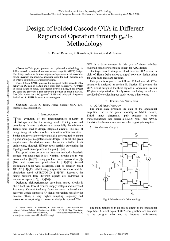
The advantages of implementing folded cascode OTA are low noise high gain high output voltage swing and also better Power Supply Rejection Ratio PSRR 20 21 23 24. Abstract This paper presents a design of the Folded-cascode operational amplifier using 125µm CMOS technology which leads to high gain as compared to a normal cascode circuit. Also the design of Folded Cascode OTA which works for frequencies that lead to a baseband circuit design for RF application is based on transistor sizing methodology.
Using 035µm CMOS process the designed folded cascode OTA achieves a DC gain of 775dB and a unity-gain frequency of 430MHz in strong inversion mode. Nr Characteristics Specification values 1 Open loop Gain 100 dB 2 Gain Bandwidth 10 MHz 3 Phase margin 60 4 Settling Time 1 µs e t a R w e l 5S 200 Vµs 6 Offset 5 µV 7 Input CMR 6 V. In a folded-cascode design such as the one used by Sock-alingam and Thibodeau there is an input differential pair and two separate current branches for the differential output.
1 Differential Input Stage 2 Folded Cascode Load Stage 3 Output Stage There are variety of structures available for all of the above three mentioned stages each have some advantages and some disadvantages of its own. In order to tailor the op amp to a particular application it has to satisfy conditions on the gain stability bandwidth slew rate noise etc. Closed-form expressions are developed and a sequence of design steps is established.
Using 035µm CMOS process the designed folded cascode OTA achieves a DC gain of 775dB and a unity-gain frequency of 430MHz in strong inversion mode. For 17mW at 3V a 05 m CMOS OTA achieves 630MHz with 51 phase margin. In this paper an enhanced IRFC EIRFC OTA is proposed by adopting the technique proposed in 3- 4 for the FC OTA.
An attempt is made to formalize the design of a fully differential folded-cascode amplifier for switched-capacitor applications by establishing design equations and procedures to assist in this process. Closed-form expressions are developed and a sequence of design steps is established. The modulator consumes 28mW at 3V and has a dy-modulator for GSM.
A1 gmi ro Equation 1 where gmi is the transconductance of the input transistor M1 and M2 and ro is the output impedance seen at the output of the OTA. I would recommend you refer to maloberti. Detailed design procedure and hand calculations The low frequency gain of the first stage the folded-cascode OTA can be written as.
Is analyzed and the results are presented in the form of design equations and procedures. Status Not open for further replies. Simulation results are performed using CADENCE software and virtuoso spectre model for CMOS 018μm process technology.
The designed folded-cascode OTA are implemented in 013µm CMOS process with BSIM3V3 level 49 MOSFET model and simulation results are performed using SPICE software. A fully differential folded-cascode op. By cascoding current mirror load at the output node the folded cascode OTA obtains higher voltage gain than the symmetrical OTA topology.
The PSRR power supply rejection ratio is also improved. In moderate inversion mode it has a 92dB DC. Tradeoffs among such factors as bandwidth gain phase margin bias currents signal swing slew rate and power are made evident.
Section IV gives design window. The amplifier consumes less than 65µA bias current at 175C. An optimum OTA topology is done in order to optimize MOS transistor sizing.
It is designed to have 25 dB of gain and approximately 70 degrees of phase margin. Design Considerations A telescopic OTA was used because of its simplicity over other designs allowing for higher-speed operation. Up to 10 cash back In this paper a new methodology for design of folded cascode FC and recycling folded cascode RFC OTAs based on 1f noise reduction is presented.
Folded cascode OTA structure is analyzed in section II. Section III presents the OTA circuit design in the three regions of operation. This OTA is referred to as Recycling Folded Cascode RFC.
From it is found that designed folded cascode OTA has a 5399dB DC gain around 351 MHz unity gain bandwidth and 53 phase margin. A fully differential folded-cascode op. Tradeoffs among such factors as bandwidth gain phase margin bias currents signal swing slew rate and power are made evident.
Understanding the design of a folded cascode OTA. A on-chip temperature stable current reference is employed to bias the amplifier. The design is done in different regions of operation weak inversion strong inversion and moderate inversion using the gmIDmethodology in order to optimize MOS transistor sizing.
The use of silicon-carbide as a material for integrated circuits ICs is gaining popularity due to its ability to function at high temperatures outside the range of typical silicon ICs. Start date Jun 3 2011. With a new formulation for input referred flicker noise based on GmId characteristic in all operation regions significantly enhance of the noise performance is achieved.
Description Of Design Stages The folded cascode operational amplifier implemented has three stages. Is analyzed and the results are presented in the form of design equations and procedures. These qualifications were met and the layout was successfully created and fabricated.
Jun 3 2011 1 B. Design of an folded cascode operational amplifier using a new high voltage technology H35 20 V Meeting these specifications Î S.

Schematic Of Folded Cascode Ota A 1 Optimized For Noise And Power Download Scientific Diagram
Design Of Folded Cascode Ota In Different Regions Of Operation

Design And Analysis Of Folded Cascode Otas Using Gm Id Methodology Based On Flicker Noise Reduction Springerlink
Design Of Folded Cascode Ota In Different
Figure 1 From An Enhanced Folded Cascode Ota With Push Pull Input Stage Semantic Scholar

Folded Cascode Ota Design For Wide Band Applications Semantic Scholar

Op Amp Topologies Folded Cascode Download Scientific Diagram

The Proposed Enhanced Phase Margin Folded Cascode Amplifier Download Scientific Diagram
0 comments
Post a Comment